
An Operational amplifier ("op-amp") is a DC-coupled high-gain electronic voltage amplifier with a differential input and, usually, a single-ended output. An op-amp produces an output voltage that is typically hundreds of thousands times larger than the voltage difference between its input terminals.
Operational amplifiers are important building blocks for a wide range of electronic circuits. They had their origins in analog computers where they were used in many linear, non-linear and frequency-dependent circuits. Their popularity in circuit design largely stems from the fact the characteristics of the final elements (such as their gain) are set by external components with little dependence on temperature changes and manufacturing variations in the op-amp itself.
Op-amps are among the most widely used electronic devices today, being used in a vast array of consumer, industrial, and scientific devices.
Circuit notation

The circuit symbol for an op-amp is shown to the right, where:
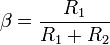
- V+ : non-inverting input
- V- : inverting input
- Vout : output
- Vs+: positive power supply
- Vs-: negative power supply
The power supply pins (Vs+ and Vs-) can be labeled in different ways. Despite different labeling, the function remains the same - to provide additional power for amplification of the signal. Often these pins are left out of the diagram for clarity, and the power configuration is described or assumed from the circuit.
Operation
The amplifier's differential inputs consist of a V+ input and a V- input, and ideally the op-amp amplifies only the difference in voltage between the two, which is called the differential input voltage. The output voltage of the op-amp is given by the equation,

where V+ is the voltage at the non-inverting terminal, V- is the voltage at the inverting terminal and AOL is the open-loop gain of the amplifier. (The term "open-loop" refers to the absence of a feedback loop from the output to the input).

Typically the op-amp's very large gain is controlled by negative feedback, which largely determines the magnitude of its output ("closed-loop") voltage gain in amplifier applications, or the transfer function required (in analog computers). Without negative feedback, and perhaps with positive feedback for regeneration, an op-amp acts as a comparator. High input impedance at the input terminals and low output impedance at the output terminal(s) are important typical characteristics.
With no negative feedback, the op-amp acts as a comparator. The inverting input is held at ground (0 V) by the resistor, so if the Vin applied to the non-inverting input is positive, the output will be maximum positive, and if Vin is negative, the output will be maximum negative. Since there is no feedback from the output to either input, this is an open loop circuit. The circuit's gain is just the GOL of the op-amp.

Adding negative feedback via the voltage divider Rf,Rg reduces the gain. Equilibrium will be established when Vout is just sufficient to reach around and "pull" the inverting input to the same voltage as Vin. As a simple example, if Vin = 1 V and Rf = Rg, Vout will be 2 V, the amount required to keep V– at 1 V. Because of the feedback provided by Rf,Rg this is a closed loop circuit. Its over-all gain Vout / Vin is called the closed-loop gain ACL. Because the feedback is negative, in this case ACL is less than the AOL of the op-amp.
The magnitude of AOL is typically very large—10,000 or more for integrated circuit op-amps—and therefore even a quite small difference between V+ and V- drives the amplifier output nearly to the supply voltage. This is called saturation of the amplifier. The magnitude of AOL is not well controlled by the manufacturing process, and so it is impractical to use an operational amplifier as a stand-alone differential amplifier. If predictable operation is desired, negative feedback is used, by applying a portion of the output voltage to the inverting input. The closed loop feedback greatly reduces the gain of the amplifier. If negative feedback is used, the circuit's overall gain and other parameters become determined more by the feedback network than by the op-amp itself. If the feedback network is made of components with relatively constant, stable values, the unpredictability and inconstancy of the op-amp's parameters do not seriously affect the circuit's performance.
If no negative feedback is used, the op-amp functions as a switch or comparator.
Positive feedback may be used to introduce hysteresis or oscillation.
Ideal and real op-amps

An equivalent circuit of an operational amplifier that models some resistive non-ideal parameters.
An ideal op-amp is usually considered to have the following properties, and they are considered to hold for all input voltages:
- Infinite open-loop gain (when doing theoretical analysis, a limit may be taken as open loop gain AOL goes to infinity)
- Infinite voltage range available at the output (vout) (in practice the voltages available from the output are limited by the supply voltages Vs+and Vs-)
- Infinite bandwidth (i.e., the frequency magnitude response is considered to be flat everywhere with zero phase shift).
- Infinite input impedance (so, in the diagram, Rin=∞, and zero current flows from V+to V-)
- Zero input current (i.e., there is assumed to be no leakage or bias current into the device)
- Zero input offset voltage (i.e., when the input terminals are shorted so that V+ = V- , the output is a virtual ground or vout = 0).
- Infinite slew rate (i.e., the rate of change of the output voltage is unbounded) and power bandwidth (full output voltage and current available at all frequencies).
- Zero output impedance (i.e., Rout = 0, so that output voltage does not vary with output current)
- Zero noise
- Infinite Common-mode rejection ratio (CMRR)
- Infinite Power supply rejection ratio for both power supply rails.
In practice, none of these ideals can be realized, and various shortcomings and compromises have to be accepted. Depending on the parameters of interest, a real op-amp may be modeled to take account of some of the non-infinite or non-zero parameters using equivalent resistors and capacitors in the op-amp model. The designer can then include the effects of these undesirable, but real, effects into the overall performance of the final circuit. Some parameters may turn out to have negligible effect on the final design while others represent actual limitations of the final performance, that must be evaluated.
Real operational amplifiers suffer from several non-ideal effects:
· Finite gain
Open-loop gain is infinite in the ideal operational amplifier but finite in real operational amplifiers. Typical devices exhibit open-loop DC gain ranging from 100,000 to over 1 million. So long as the loop gain (i.e., the product of open-loop and feedback gains) is very large, the circuit gain will be determined entirely by the amount of negative feedback (i.e., it will be independent of open-loop gain). In cases where closed-loop gain must be very high, the feedback gain will be very low, and the low feedback gain causes low loop gain; in these cases, the operational amplifier will cease to behave ideally.
· Finite input impedances
The differential input impedance of the operational amplifier is defined as the impedance between its two inputs; the common-mode input impedance is the impedance from each input to ground. MOSFET-input operational amplifiers often have protection circuits that effectively short circuit any input differences greater than a small threshold, so the input impedance can appear to be very low in some tests. However, as long as these operational amplifiers are used in a typical high-gain negative feedback application, these protection circuits will be inactive. The input bias and leakage currents described below are a more important design parameter for typical operational amplifier applications.
· Non-zero output impedance
Low output impedance is important for low-impedance loads; for these loads, the voltage drop across the output impedance of the amplifier will be significant. Hence, the output impedance of the amplifier limits the maximum power that can be provided. In a negative-feedback configuration, the output impedance of the amplifier is effectively lowered; thus, in linear applications, op-amps usually exhibit a very low output impedance indeed. Negative feedback can not, however, reduce the limitations that Rload in conjunction with Rout place on the maximum and minimum possible output voltages; it can only reduce output errors within that range.
Low-impedance outputs typically require high quiescent (i.e., idle) current in the output stage and will dissipate more power, so low-power designs may purposely sacrifice low output impedance.
· Input current
Due to biasing requirements or leakage, a small amount of current (typically ~10 nanoamperes for bipolar op-amps, tens of picoamperes for JFET input stages, and only a few pA for MOSFET input stages) flows into the inputs. When large resistors or sources with high output impedances are used in the circuit, these small currents can produce large unmodeled voltage drops. If the input currents are matched, and the impedance looking out of both inputs are matched, then the voltages produced at each input will be equal. Because the operational amplifier operates on the difference between its inputs, these matched voltages will have no effect (unless the operational amplifier has poor CMRR, which is described below). It is more common for the input currents (or the impedances looking out of each input) to be slightly mismatched, and so a small offset voltage can be produced. This offset voltage can create offsets or drifting in the operational amplifier. It can often be nulled externally; however, many operational amplifiers include offset null or balance pins and some procedure for using them to remove this offset. Some operational amplifiers attempt to nullify this offset automatically.
· Input offset voltage
This voltage, which is what is required across the op-amp's input terminals to drive the output voltage to zero, is related to the mismatches in input bias current. In the perfect amplifier, there would be no input offset voltage. However, it exists in actual op-amps because of imperfections in the differential amplifier that constitutes the input stage of the vast majority of these devices. Input offset voltage creates two problems: First, due to the amplifier's high voltage gain, it virtually assures that the amplifier output will go into saturation if it is operated without negative feedback, even when the input terminals are wired together. Second, in a closed loop, negative feedback configuration, the input offset voltage is amplified along with the signal and this may pose a problem if high precision DC amplification is required or if the input signal is very small.
· Common mode gain
A perfect operational amplifier amplifies only the voltage difference between its two inputs, completely rejecting all voltages that are common to both. However, the differential input stage of an operational amplifier is never perfect, leading to the amplification of these identical voltages to some degree. The standard measure of this defect is called the common-mode rejection ratio (denoted CMRR). Minimization of common mode gain is usually important in non-inverting amplifiers (described below) that operate at high amplification.
· Temperature effects
All parameters change with temperature. Temperature drift of the input offset voltage is especially important.
· Power-supply rejection
The output of a perfect operational amplifier will be completely independent from ripples that arrive on its power supply inputs. Every real operational amplifier has a specified power supply rejection ratio (PSRR) that reflects how well the op-amp can reject changes in its supply voltage. Copious use of bypass capacitors can improve the PSRR of many devices, including the operational amplifier.
· Drift
Real op-amp parameters are subject to slow change over time and with changes in temperature, input conditions, etc.
· Noise
Amplifiers generate random voltage at the output even when there is no signal applied. This can be due to thermal noise and flicker noise of the devices. For applications with high gain or high bandwidth, noise becomes a very important consideration.
Classification
Op-amps may be classified by their construction:
- discrete (built from individual transistors or tubes/valves)
- IC (fabricated in an Integrated circuit) - most common
- hybrid
IC op-amps may be classified in many ways, including:
- Military, Industrial, or Commercial grade (for example: the LM301 is the commercial grade version of the LM101, the LM201 is the industrial version). This may define operating temperature ranges and other environmental or quality factors.
- Classification by package type may also affect environmental hardiness, as well as manufacturing options; DIP, and other through-hole packages are tending to be replaced by Surface-mount devices.
- Classification by internal compensation: op-amps may suffer from high frequency instability in some negative feedback circuits unless a small compensation capacitor modifies the phase- and frequency- responses; op-amps with capacitor built in are termed "compensated", or perhaps compensated for closed-loop gains down to (say) 5, others: uncompensated.
- Single, dual and quad versions of many commercial op-amp IC are available, meaning 1, 2 or 4 operational amplifiers are included in the same package.
- Rail-to-rail input (and/or output) op-amps can work with input (and/or output) signals very close to the power supply rails.
- CMOS op-amps (such as the CA3140E) provide extremely high input resistances, higher than JFET-input op-amps, which are normally higher than bipolar-input op-amps.
- other varieties of op-amp include programmable op-amps (simply meaning the quiescent current, gain, bandwidth and so on can be adjusted slightly by an external resistor).
- manufacturers often tabulate their op-amps according to purpose, such as low-noise pre-amplifiers, wide bandwidth amplifiers, and so on.
Applications

Basic single stage amplifiers
Non-inverting amplifier

An op-amp connected in the non-inverting amplifier configuration
In a non-inverting amplifier, the output voltage changes in the same direction as the input voltage.
The gain equation for the op-amp is:

However, in this circuit V– is a function of Vout because of the negative feedback through the R1R2 network. R1 and R2 form a voltage divider, and as V– is a high-impedance input, it does not load it appreciably. Consequently:

where
Substituting this into the gain equation, we obtain:

Solving for Vout:

If AOL is very large, this simplifies to

Inverting amplifier

An op-amp connected in the inverting amplifier configuration
In an inverting amplifier, the output voltage changes in an opposite direction to the input voltage.
As for the non-inverting amplifier, we start with the gain equation of the op-amp:

This time, V– is a function of both Vout and Vin due to the voltage divider formed by Rf and Rin. Again, the op-amp input does not apply an appreciable load, so:

Substituting this into the gain equation and solving for Vout:

If AOL is very large, this simplifies to

A resistor is often inserted between the non-inverting input and ground (so both inputs "see" similar resistances), reducing the input offset voltage due to different voltage drops due to bias current, and may reduce distortion in some op-amps.
A DC-blocking capacitor may be inserted in series with the input resistor when a frequency response down to DC is not needed and any DC voltage on the input is unwanted. That is, the capacitive component of the input impedance inserts a DC zero and a low-frequency pole that gives the circuit a bandpass or high-pass characteristic.
Positive feedback configurations
Another typical configuration of op-amps is the positive feedback, which takes a fraction of the output signal back to the non-inverting input. An important application of it is the comparator with hysteresis (i.e., the Schmitt trigger).
Other applications
- audio- and video-frequency pre-amplifiers and buffers
- voltage comparators
- differential amplifiers
- differentiators and integrators
- filters
- precision rectifiers
- precision peak detectors
- voltage and current regulators
- analog calculators
- analog-to-digital converters
- digital-to-analog converter
- voltage clamps
- oscillators and waveform generators
Internal circuitry of 741 type op-amp
Though designs vary between products and manufacturers, all op-amps have basically the same internal structure, which consists of three stages:
A component level diagram of the common 741 op-amp. Dotted lines outline: current mirrors (red); differential amplifier (blue); class A gain stage (magenta); voltage level shifter (green); output stage (cyan).
- Differential amplifier – provides low noise amplification, high input impedance, usually a differential output.
- Voltage amplifier – provides high voltage gain, a single-pole frequency roll-off, usually single-ended output.
- Output amplifier – provides high current driving capability, low output impedance, current limiting and short circuit protection circuitry.
Note: while the 741 was historically used in audio and other sensitive equipment, such use is now rare because of the improved noise performance of more modern op-amps. Apart from generating noticeable hiss, 741s and other older op-amps may have poor common-mode rejection ratios and so will often introduce cable-borne mains hum and other common-mode interference, such as switch 'clicks', into sensitive equipment.
The "741" has come to often mean a generic op-amp IC (such as uA741, LM301, 558, LM324, TBA221 - or a more modern replacement such as the TL071). The description of the 741 output stage is qualitatively similar for many other designs (that may have quite different input stages), except:
- Some devices (uA748, LM301, LM308) are not internally compensated (require an external capacitor from output to some point within the operational amplifier, if used in low closed-loop gain applications).
- Some modern devices have rail-to-rail output capability (output can be taken to positive or negative power supply rail within a few millivolts).