Now that you are familiar with the combinational logic circuits, you would know that these circuits give the required outputs but cannot store them. In other words, the combinational logic circuits are memory less.Hence we can say that the output of the combinational circuit depends only on the present input/present state. So don't you think this is analogous to our SGPA?


![]()

On the other hand, the sequential logic circuits are said to have an inbuilt memory. So they can remember their previous state. Therefore the output of a sequential logic circuit depends on the present input as well as on the previous output. So wondering how they have such a good memory?? It is because they contain storage elements!! we can say that..
Needless to say , isn't it similar to CGPA? Let us now try to picturise how a sequential circuit would look like. The block diagram below will help you.
About the memory elements..
Wanna know what these memory elements are we were talking about all this while?
A memory element is a circuit which consists of a periodic clock signal as one of it's inputs. It stores or latches within itself the input applied to it until the clock signal changes it's state.
The word sequential means that things happen in a sequence, one after another and in sequential logic circuits, the actual clock signals determines when things will happen next.
Classification of sequential logic circuits..
Comparison between the two..
So why is it heavier on the side of synchronous circuits?
Because of the following.,
Advantages of the synchronous circuits..
- Faster operation
- Ease of avoiding problems due to hazards
- Lower hardware requirement
- Better noise immunity
- Latches
- Flip flops
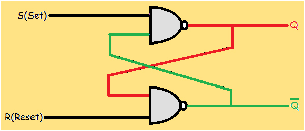
It has two outputs Q and Q', which are always complements of each other.
In SET state, Q is HIGH (logic 1) and Q' is LOW (logic 0) whereas in RESET state, Q is LOW (logic 0) and Q' is HIGH (logic 1).
For a flip flop to act as a memory device, it should retain the information stored in it. Thus if it is in SET state, it should remain in SET state and if it is in RESET state, it should remain in RESET state.
S R Latch using NOR gates..
It can be observed from the figure, that an SR latch is made up of two cross coupled NOR gates. The latch has two inputs, S for SET and R for RESET and two outputs, Q and Q' which are complements of each other.
Truth table
S R Q Q' Comments
1 0 1 0 SET state
0 0 1 0 No change
0 1 0 1 RESET state
0 0 0 1 No change
1 1 0 0 Undefined
It is seen that when both the inputs are equal to 1, an undefined state occurs with both the outputs equal to 0.
An SR latch can also be implemented using NAND gate as shown below.
S R Latch using NAND gates..
Truth table
S R Q Q' Comments
0 1 1 0 SET state
1 1 1 0 No change
1 0 0 1 RESET state
1 1 0 1 No change
0 0 1 1 Undefined
Here when both the inputs are equal to 1 at the same time, an undefined state occurs with both the outputs equal to 1.
So how do we eliminate this undefined state?? This is done in the D latch.
D latch..
A D latch has two inputs, D(Data) and C(Control). The complement of the D is applied to the S' input and D is directly applied to the R' input. This the disadvantage of an SR latch is overcome. As long as C=0, regardless of the value of D, the output remains unchanged. Once C=1, the output follows the input D. In other words, the data D is transferred to the output. Hence the name data transfer latch or D latch.
Replace the control input C with a periodic clock signal and look what you have.. D flip flop!!
Truth table
C D Qn+1 Comments
0 x Qn No change
1 0 0 Data transferred
1 1 1 Data transferred
0 x Qn No change
1 0 0 Data transferred
1 1 1 Data transferred
Hey isn't it same as the truth table of a mod 2 counter?? Yes, one which counts 0 and 1!
So now let's move on to T flip flop.
T Flip flop..
Just remove the NOT gate from the D flip flop and you obtain a T flip flop. As simple as that! Similar to the D version of it, this too has two inputs, T and control input C. As long as C=0, irrespective of the value of T, there is no change in the output. Once C=1, the flip flop retains the same state if T=0 and if T=1, the output of the flip flop toggles. Hence the name Toggle flip flop or T flip flop.
Truth table
C T Qn+1 Comments
0 x Qn No change
1 0 Qn No change
1 1 Q'n Toggles
0 x Qn No change
1 0 Qn No change
1 1 Q'n Toggles
Both D and T flip flops are used in the construction of counters which we will come across in sometime.
J K Flip flop..
The above mentioned limitation of the SR flip flop could be overcome using JK flip flop as well. It is the most widely used flip flop. Also known as the universal flip flop circuit since it is possible to obtain other flip flops from JK flip flop. The operation of JK flip flop is same as that of the SR flip flop. The only difference is the addition of a clock input circuitry that prevents the invalid output condition that occurs when S=R=1. The S and R inputs are now replaced by J and K named after its inventor Jack Kilby.
It consists of two 3 input NAND gates with the third input of each gate connected to the outputs Q and Q'. This cross coupling allows the previously invalid input states to be used to produce a toggle condition. So this is how the truth table looks like.
Truth table
J K Q Q' Comments
1 0 1 0 SET state
0 0 1 0 No change
0 1 0 1 RESET state
0 0 0 1 No change
1 1 1 0 Toggles --> Note the difference
Master Slave flip flops..
SR master slave flip flop..
This is what it contains. Two SR latches with control input and an inverter. The left clocked SR latch is the master and the right one the lave. Let us find out why they are called so. So here it goes. When the clock input C=0, the output of the inverter is at logic 1 and hence the SR latch on the right is enabled. Therefore its output is same as the output of the master Y. In other words it follows the master and hence the slave.
When the clock input C=1, the master is enabled and since the output of inverter is 0, the slave is disabled. In this condition, the values of S and R affect the output Y of the master. Thus it reflects any changes any change in the values of the applied inputs. Since the slave is now disabled, it remains in the same state and any change in the output of the master goes unnoticed by the slave.
When C returns to 0, once again the master is disabled and the slave is enabled. It now transmits the present value of Y as the output Q.
JK master slave flip flop..
It is made up of clocked SR latched. The output of the first one called the master is given as input to the second which is the slave. The outputs of the slave is fed back to inputs of the master. When the clock input C=1, the output of the inverter goes low. This enables the master and the slave remains disabled. The master functions like a JK flip flop and the output appears at the input of the slave. Since the slave is inactive, the output Q remains unchanged.
When C=0, the master is disabled and the slave is enabled. This slave now functions like an SR flip flop and its output changes which is also applied to the input of the master.
When returns to 1, the master is enabled and the output is transmitted to Q when the clock once again goes low.
it is called the master slave flip flop because the master decides the output, which is simply latched out by the slave.
Positive edge triggered D flip flop..
As the name suggests, it ignores the clock pulse when it is a constant level and gets triggered only during the 0 to 1 transition of the or during the positive edge of the clock pulse.
A positive edge triggered D flip flop is basically a master slave flip flop with the master being a D flip flop and slave being an SR latch. When a negative edge of the clock input occurs, master is enabled and follows the D input value whereas the slave is disabled. Therefore the output remains unchanged.
When a positive edge occurs, the output of the inverter goes high. Thus the master is disabled and the slave is enabled. The slave now copies the master. Thus the state of the master at the positive edge of the clock pulse is copied by the slave.
About the direct inputs..
There are two types of direct inputs.
- Preset or direct set - Asynchronously sets the flip flop.
- Clear or direct reset - Asynchronously resets the flip flop.
Counters..
What is a counter supposed to do?? It's so obvious. It is a circuit that counts the number of occurrences of an input. For example., it counts the number of clock pulses.
Classification of counters..
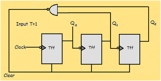
4 bit binary ripple counter..
The above figure shows a 4 bit binary asynchronous counter. It consists of 4 T flip flops. The output Q of one is fed to the clock input of the next. It can be seen that for every negative transition of the input clock, the output Q0 toggles. Similarly, for every negative transition of Q0, Q1 toggles and so on for Q2 and Q3.
Thus the outputs Q3, Q2, Q1, Q0 change in increasing sequence from 0000 through 1111. After 15th pulse, they reset back to 0000 and the count begins again. It is an up counter because the count sequence is in increasing order.
Truth table
Clock pulses Q3 Q2 Q1 Q0
0 0 0 0 0
1 0 0 0 1
2 0 0 1 0
3 0 0 1 1
4 0 1 0 0
5 0 1 0 1
6 0 1 1 0
7 0 1 1 1
8 1 0 0 0
9 1 0 0 1
1 0 1 0 1 0
11 1 0 1 1
12 1 1 0 0
13 1 1 0 1
14 1 1 1 0
15 1 1 1 1
Mod n counters..
A mod n counter is one which counts pulses from 0 to n-1. In a mod n counter, all the output bits should be reset or Q=0000 after the (n-1)th input pulse. In order to do this, the output bits corresponding to to the (n-1)th input pulse which need to be reset are given as inputs to a NAND gate and the output of the NAND gate is fed to the clear inputs of the flip flops. Got confused?? The following example of a mod 6 counter will make it much simpler.
Mod 6 counter..
Truth table
Clock pulses Q2 Q1 Q0
0 0 0 0
1 0 0 1
2 0 1 0
3 0 1 1
4 1 0 0
5 1 0 1
6 0 0 0
6 0 0 0
A mod 6 counter should count from 0 through 5 i.e, from Q=000 to 101. After counting the 5th pulse, the output should reset to 000. For the 6th pulse, Q2=1, Q1=1 and Q0=0. In order to reset the input, Q2 and Q1 should be made 0. Thus Q2 and Q1 are given as inputs to a NAND gate. Since both the inputs to the NAND gate are 1's, the output of the gate is 0. This output is then applied to the clear inputs of all 3 T flip flops which in turn resets the flip flops and hence Q=000. It then again starts counting from 1 and so on..